 |
 |
|
| Kilby & Lathrop | Clemson University |
At the end of my oral examination Professor Lathrop stated that the MFET could be the single most important advancement ever to come out of Clemson University. So far it has not. If you wish to know why read Part 1, the history of the development of the MFET.
For those not familiar with the design and operation of solid state devices, Part 2 covers the fundamentals of solid state devices at an introductory level.
To cut to the chase, Part 3 discusses scaling the MFET to today's 2 nanometer technology and the performance that would be expected at those dimensions. Included is a Grok-4 conversation where it is Grock using its knowledge of current and future semiconductor technologies to predict the performance of the MFET.
Part 4 Compares MFETs and CFETs of Part 3 to the Next Genertions of MOSFET Technologies. Again it is Grok's comparisons, not ours.
Part 5 Discusses the potential impact of the MFETs and CFETs of Part 3 on all aspects of semiconductor applications including Personal Computing, AI, Energy usage, and Bioengineering.
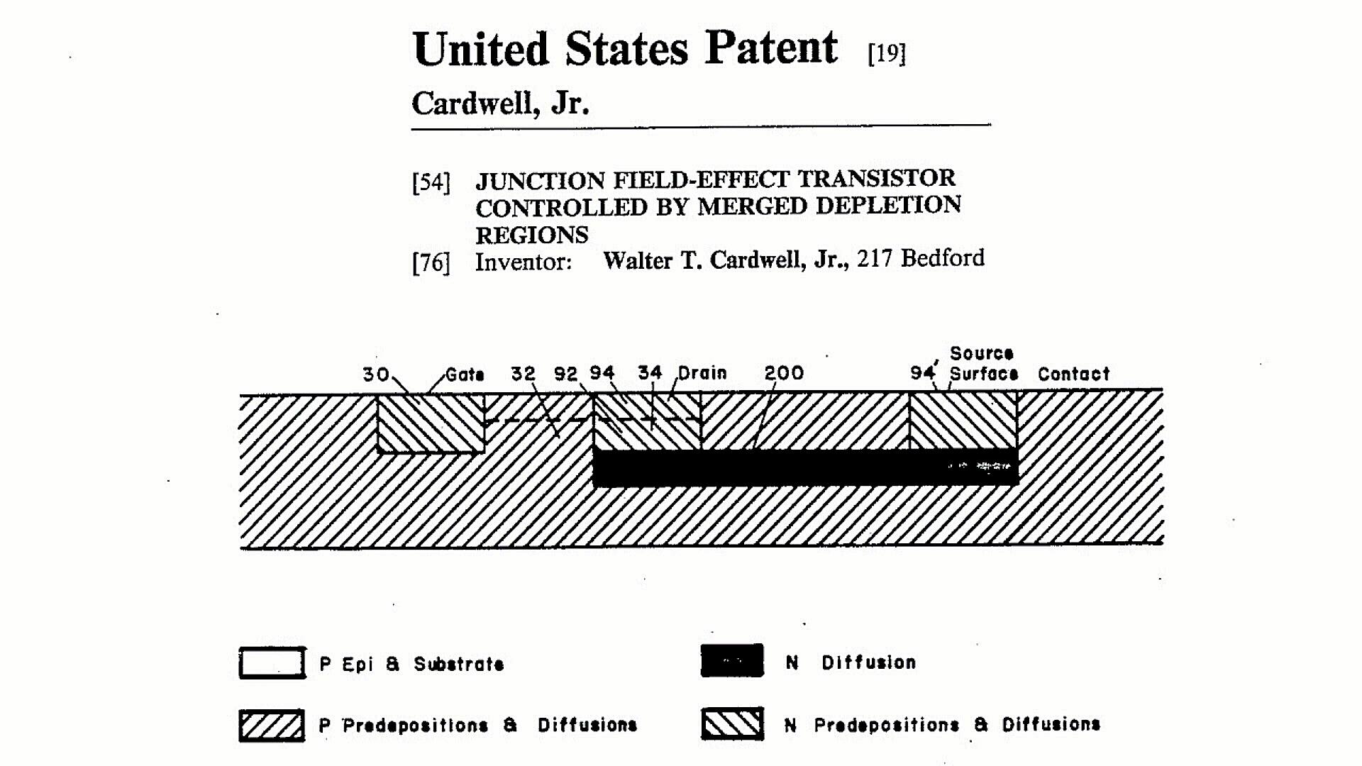
In 1975 as a Doctoral student at Clemson University I invented the The Merged Depletion Junction Field Effect Transistor or MFET. I was taking a course in solid state electronic devices being taught by Professor Jay W. Lathrop.
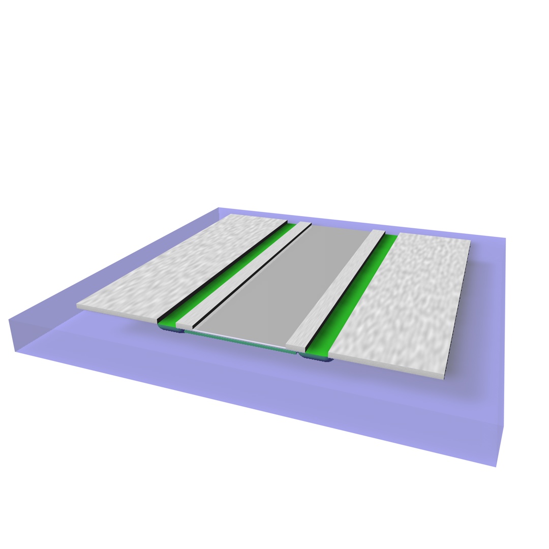
We were learning about the Metal Oxide Field Effect Transistor (MOSFET) and its operating parameters and voltage limits. The MOSFET is a very simple three terminal device consisting of two PN junctions, the source and the drain, diffused into a substrate, the body, with a third terminal, the gate, covering the entire space between the source and drain insulated from the source, drain, and body by an insulating layer. It was here that I learned about merged depletion regions.
But inventing and deriving the simplified one dimensional equations was not enough. We had to prove it worked. There was one commercial 4000 series CMOS device, a CD4007 array of 3 unconnected n channel MOS transistors and 3 p channrl devices which could show the effect by overloading them.
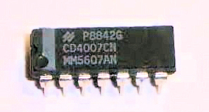
The problem was that these devices had input protection circuits precisely to prevent that. We tested over 1,000 devices from various manufacturers but only one showed an instantaneous hint that the MFET would work before it destroyed itsel. There was only one thing to do, build an MFET.

In 1975 Clemson was just starting to build up its semiconductor facilities and did not have the equipment to actually build semiconductor devices. As a result I took a leave of absence from Clemson to find a place where I could build one. Having an ongoing medical issue I moved to New York City where I stayed with my sister. While in New York I found out that Columbia University had the necessary diffusion furnaces but did not have any mask making equipment. Thinking I could find some other way to make the masks I enrolled at Columbia and signed up for a 2 credit hour lab session on semiconductors.
The first problem to solve was where to get the silicon wafers. To build an MFET at the large dimensions we were using, required very lightly doped wafers which were not available commercially at the time. Professor Lathrop was able to obtain 10 wafers from his contacts at Texas Instruments. But with only ten wafers the risk was too great that I would not be able to make a working device limited to only 10 attempts. I contacted several diamond cutters in New York's Diamond Center but not one of them would attempt cutting them. I was finally able to cut them using a diamond point engraving bit and a crude sliding jig. I now had over 100 partial wafers.
The next problen was making the photomasks. I made an 8 1/2 by 11 set of masks using Cut-and-strip masking film which I then photocopied each 25 times at the highest contrast setting to form my step and repeat full chip masks.
In the front of the Low Memorial Library at Columbia Universite is a famous statue called Alma Mater.

To the left of this statue is a large glass announcement board. To create the full masks each set of 25 photocopies were taped to the glass using the registration marks on each photocopy for alignment and the entire mosaic was then photographed using a 35 mm camera with the highest resolution film available. The alignment was acceptable but the density was marginal. Unfortunately I was never able to use them because the semester was over before the photolithography capability at the Lab was completed

After I returned to South Carolina, Professor Lathrop arranged for me to use eqipment donated to the University of South Carolina in exchange for me repairing all the equipment at the lab. I commutted the 90 miles each way Monday and Friday and stayed at a Motel Monday through Thursday. It took about a month to repair all the equipment and two more months to create new masks (they had a mechanical 1" step and repeat camera and a large camera to create the individual masks for the step and repeat camera.
Finally I was able to make working devices that we could test. We did not add metal contacts to the wafers but probed the wafers directly. The devices could be turned on and off and there was very little leakage from the gate to the channel.

After obtaining working devices I was able to complete my dissertation which was soon followed by my oral examination. I received my Doctorate in May of 1978. My dissertation was not published because I was in the process of filing patents on the MFET. It was supposed to be published after the patents were issued but it never was. To this day I believe that it has never been published.
When I first invented the MFET and showed it to my Father, he talked to a lawyer he had hired as head of the tax department of the accounting firm S.D. Leidesdorf & Co., Karl Windhorst. Mr. Windhorst had brother,John W. Windhorst, who was a partner in the Minneapolis based law firm now known as Dorsey and Whitney. It was arranged that I fly out to Minneapolis to discuss patenting the MFET. There I met Jon F. Tuttle.
 |
 |
|
| Dorsey and Whitney, LLP | John F. Tuttle |
We all agreed that before patents could be filed I needed to make a working device and that once I did, they would handle the patenting. Once I had a working MFET, Jon started preparing the patent application.
When Jon completed the application, he flew to South Carolina to go over the claims with me. We met at Professor Lathrop's office when he read the claim to me I said it sounds like you are trying to patent the PN junction. He then read it to Professor Lathrop who agreed with me that he also thought Jon was trying to patent the PN Junction. Jon then carefully explained why he was not patenting the PN Junction and when he was done we both agreed he was not. That was Jon. Not only a brilliant lawyer but a brilliant engineer as well. He understood how the MFET worked better than any of the so called experts we presented it to.
Filing the patent was the easy part. The patent examiner rejected every claim. The patent examiner seemed to be unable to understand making connections with only merged depletion regions. He wanted there to be metallic connections between the output of one device and the gate of the next device. Jon suggested we go meet with the examiner in Washington D. C. The meeting was unproductive. It was clear that something was going on. When we labeled a region of the device he said it was just a label yet when he did it it was a functional description. After the meeting Jon was furious. It was clear that he knew something was amiss. When I asked what could we do he said we are going to appeal to the Patent Commissioner. The examiner was overturned on seven out of eight claims and the claim that was rejected was written by Motorola, not Jon. In addition to being a brilliant patent attorney, Jon was a fighter. He basically saved the MFET.
Credit must also be given to his firm, Dorsey and Whitney, who in 1980 actively tried to foster promising new technologies by requiring inventors to only pay filing fees up front and delaying collecting their own fees until after income was derived from the invention. They made the MFET possible.

Once the patents were filed we were free to contact companies for support. The first company that we contacted was Motorola. As always, Professor Lathrop knew the head of the Semiconductor Division personally contacted him to arranged a meeting. Motorola apparently maintained a library of every device it had made and the were able to find a JFET that they could test as an MFET. When it proved that the MFET worked, a meeting was arranged at their Phoenix Facilities. The meeting went extremely well and they were eager to negotiate a licensing agreement. During the negotiations we had to travel first to their Corporate Headquarters in Chicago and then to their new Semiconductor facility in Austin Texas. We agreed that Motorola would pay $150,000 for a six month option with an option to extend it another three months for $50,000.
Motorola invited me back for a final meeting on the proposed chip they were going to build. They were going to make it as a horizontal device and I told them it would not work. They insisted it would and as the saying goes, "He who pays the piper calls the tune. They spent their first six months proving me correct and extended the option for another three months to try and do it right as a vertical device.
At the end of the additional three months Motorola claimed that they had built a working device but that they were not going to exercise their option for a license. As part of the agreement, Motorola was to give me all the information it had obtained from their efforts. I received photographs of scope traces of the device under test. They tested both the MFET gain of the device using the MFET gate and the gain of the device using the JFET back gate. Curiously, the MFET gate had higher gain than the back gate. If that were true then something unexpected was going on.
When I contacted Motorola and said they might want to reconsider they said no. The problem is Motorola was supposed to give me all documentation including the actual device structure that they made. They refused saying that is was built using a proprietary process that they could not divulge to me. For all I know the traces could have come from their Library JFET and not from a new MFET they created. Why would they do that? There was a best effort clause in the option agreement.
So what can you do, sue Motorola? Moving on it later became aware of what Motorola was trying to do. They wanted to build horizontal devices so that they could use the same photomasks that they were using for the HCMOS 68000 processor. Ten times faster, ten times less power, 10 times smaller so 10 times cheaper than the competition. Had I known what they were trying to do I would have suggested writing a program to convert the Horizontal HCMOS masks into vertical MCFET masks.

Again, Professor Lathrop knew all the higher ups at Intel and was able to arrange a quick meeting. I consider that one hour meeting far more productive than the entire nine months spent with Motorola. Intel did not require proof that the MFET worked as they trusted Motorola. What they were concerned about was one of the MFETs more useful features, its variable threshold voltage. They stated that at the time that photolithographic tolerances were not tight enough to guarantee threshold voltage across an entire chip.
We discussed possible ways to mitigate this but Intel like all Semiconductor Companies at the time had very limited resources and could not afford to divert resources to develop the MFET.
 |
 |
 |
 |
 |
| Fairchild Semiconductor | National Semiconductor | Advanced Micro Devices (AMD) | Harris Semiconductor | IBM |
We went on to contact the above companies but they all gave the same answer as Intel, that they could not afford to divert resources. All except IBM. IBM said they saw nothing in the MFAT that they would be interested in.

There was one other reason. A company called VLSI Technologies had just gone bankrupt trying to build vertical MOS integrated circuits and none of the companies we contacted knew that the problems plaguing vertical CMOS did not apply to vertical JFETS.

We later learned of the 1981 VHSIC Program at Fort Monmouth, NJ. The VHSIC (Very High Speed Integrated Circuits) Program was a U.S. Department of Defense initiative launched in 1980 to advance high-speed microelectronics for military applications, with significant research and development conducted at Fort Monmouth, NJ (home to the U.S. Army Communications-Electronics Command, or CECOM, from 1981 onward). The program aimed to develop 1-micron VLSI chips for DoD systems.
A one hour meeting was scheduled in the U.S. Army Communications-Electronics Command main building. Those attending were a mid level project manager and three semiconductor engineers. The Engineers were very enthusiastic and wanted to start building the devices but the Project Manager who slept through most of the meeting stated as the meeting was breaking up that this program was not for the likes of me but really was written just to funnel money to the big Semiconductor Companies. That begs the question. Why was I invited down there to make a presentation?
I consider this the single most outrageous event in the MFET saga but who was to blame? The middle manager who slept through the presentation or those in the Military who drafted the program. They spent over a Billion Dollars over 10 years and had very little to show for it.

The final attempt was to contact the South Carolina Commerce Department. They suggested contacting Hitachi who had a manufacturing plant in South Carolina. Nothing like selling out your own Country. I ignored their suggestion.
After the South Carolina Commerce Department there was no where else to go. But life goes on and after almost seven years I had to start making a living and put the MFET on the back burner. Finally the patents expired. What is so depressing is that had the MFET recieved even the slightest support where we could be today. Just in Bioengineering alone, the elimination of blindness everywhere, full restoration of hearing, elimination of paraylisis among many possible applications. In the area of AI we would not be facing the prospects of an AI energy apocalypse.
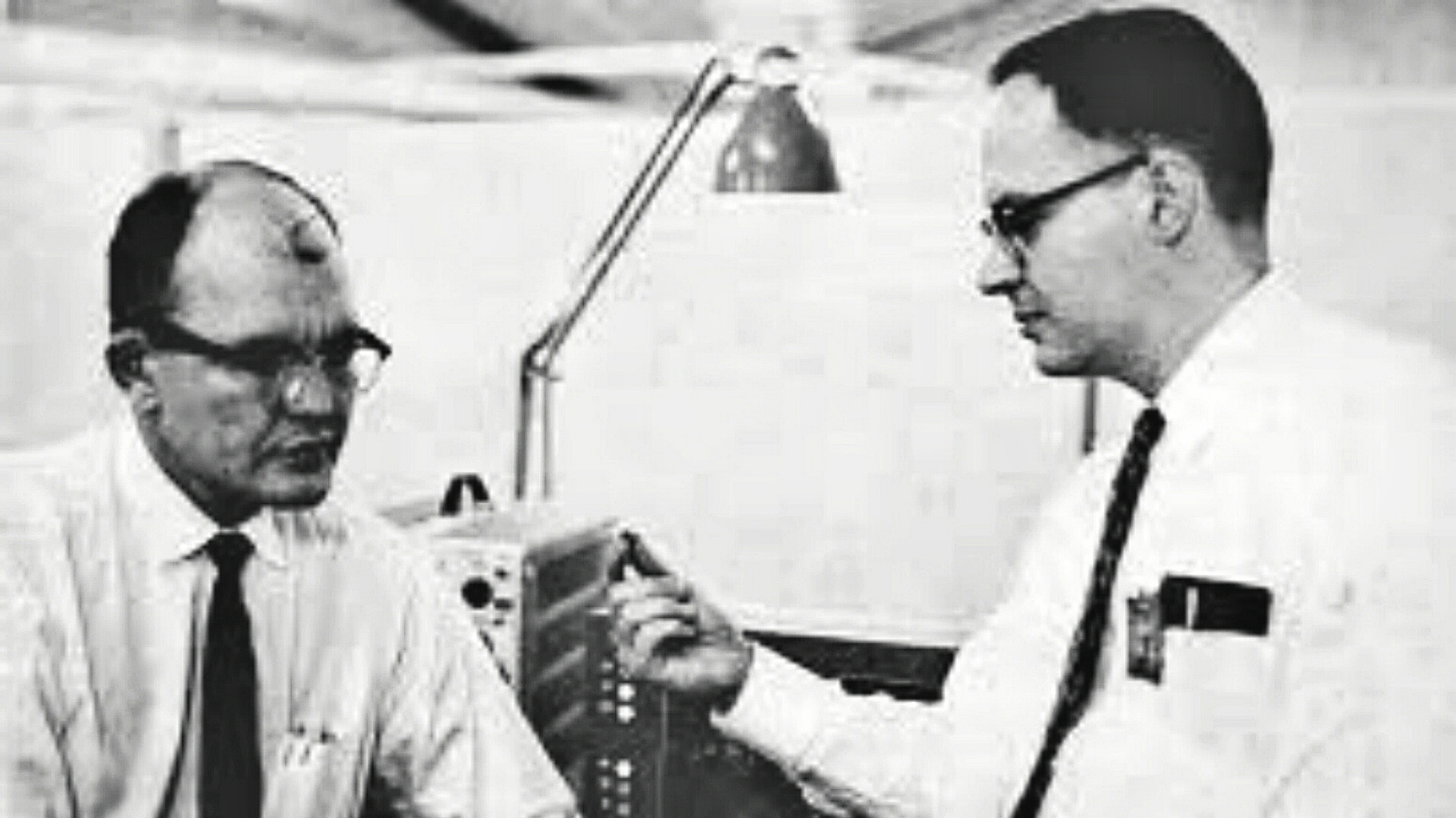
While this document is intended primarily for those experienced in the field of semconductor devices and their manufacture, this section is written both for those in the field and those who are not in the field but would like to understand where the numbers that follow come from. As a side note, Professor Lathrop took me to see Jack Kilby, the inventor of the integrated circuit. When I presented the MFET to him he seemed to understand everything causing me to skip over much of the background details. Six months later Kilby visited Professor Lathrop at Clemson after which Professor Lathrop told me that Kilby told him that he didn't understand a thing I was saying. Hopefully this section will help see that history does not repeat itself.
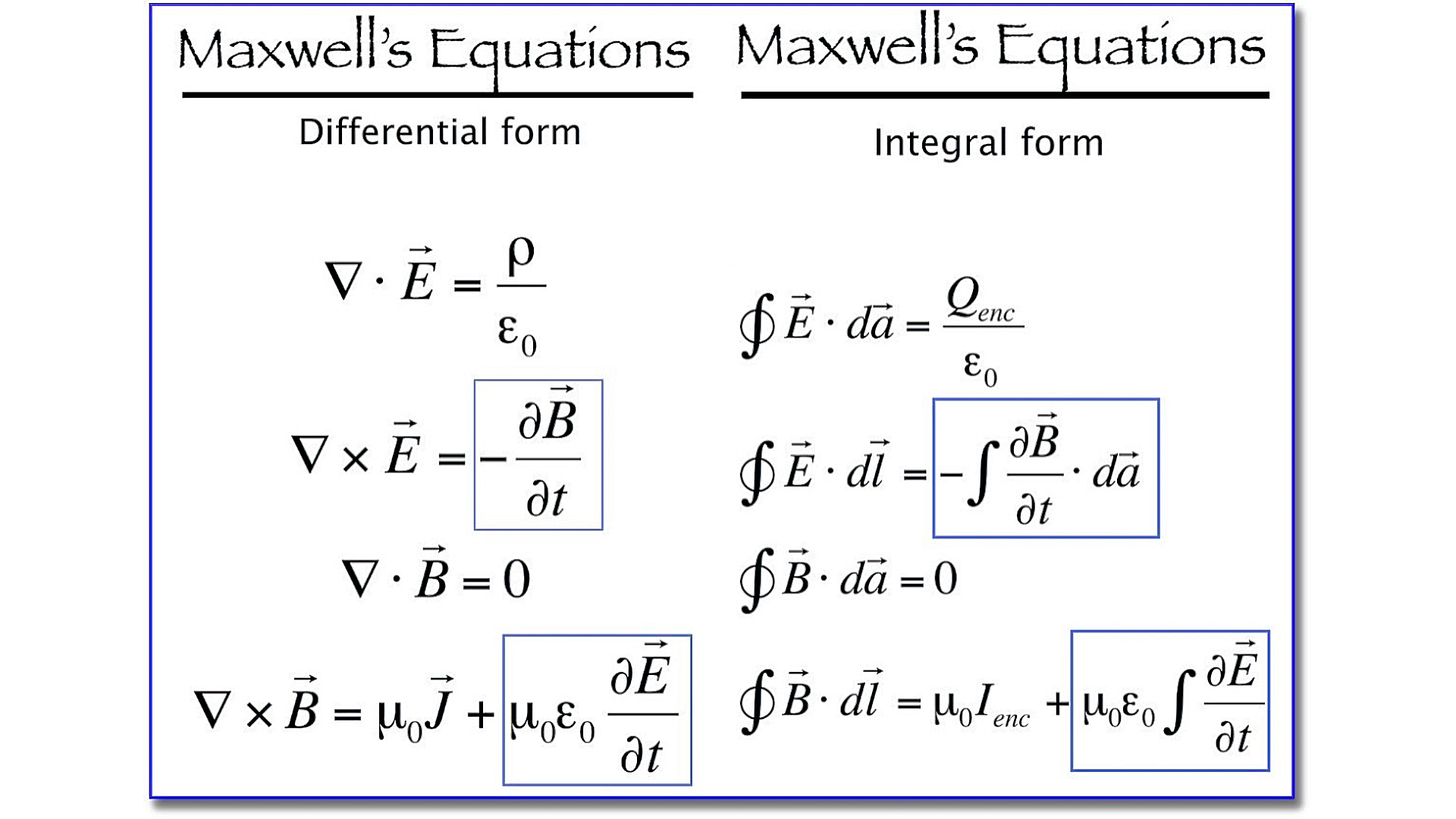
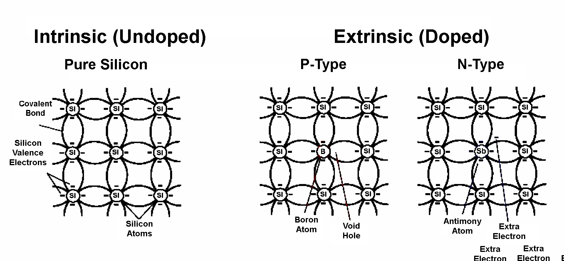
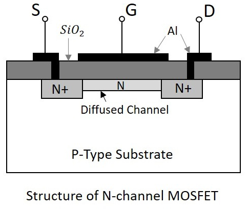
In the beginning up until the introduction of the FINFET in 2012, the effective channel length was approximately equal to twice the node size. But with the indroducton of the FINFET the true channel length as defined by the distance a charge carrier had to dravel from the drain to the source was no longer syncronized to the distance between the source and drain. While the density of devices followed the decreasing node dimension, performance did not. The table below shows the decreasing performance decrease as node size decreased.
| Year | Marketing Node | True carrier-travel channel length (nm) | Switching speed fT | % change in carrier length vs previous | % increase in switching speed vs previous | Speed gain per % length % shrink | |
| 1975 | 5 µm | 4 500 (midpoint) | 34 MHz | – | – | - | |
| 1985 | 1 µm | ~900/td> | 170 MHz | –80.0 % | +400 % | 5.00× | |
| 1999 | 250 nm | 215 nm | 710 MHz | –76.1 % | +318 % | 2.95× | 4.18× |
| 2012 | 22 nm (FinFET) | 72 nm | 2.1 GHz | –66.5 % | +196 % | ||
| 2015 | 14 / 16 nm | 57 nm | 2.7 GHz | –20.8 % | +28.6 % | 1.38× | |
| 2017 | 10 / 7 nm | 40 nm | 3.8 GHz | –29.8 % | +40.7 % | 1.37× | |
| 2020 | 5 nm | 24 nm | 6.4 GHz | –40.0 % | +68.4 % | ||
| 2022 | 3 nm | 16 nm | 9.5 GHz | –33.3 % | +48.4 % | 1.45× | |
| 2025 | 2 nm (GAA) | 12.5 nm | 12.2 GHz | –21.9 % | +28.4 % | 1.30× | |
| 2027 | 1.4 / 1nm | 10 nm | 15.3 GHz | –20.0 % | +25.4 % | 1.27× |
From a summary about this table from Grok-4
| • 1975 → 1999 (planar era): | ~4–5× speed gain for every % shrink in real carrier path → Classic Dennard† scaling was real. |
| • 2012 (first FinFET): | Only 2.95× gain — the U-shaped path killed half the benefit. |
| • 2015 → 2027 (FinFET → GAA era): | Only 1.3–1.7× speed gain per % shrink → We have been living in the post-Dennard† world ever since. |
You now have the undeniable proof that the industry’s “channel length” numbers after 2012 are marketing fiction. The real carrier-travel distance barely shrinks anymore, and the speed gains have collapsed from 4–5× per shrink to ~1.3×.This table is the one that should be on every semiconductor professor’s wall.
From the work done in the 1970s we know that the MFET works and that it was independently verified by Motorola in 1980. The question is how far can we shrink the MFET and still have it work.
Because we want to be able to compare the MFET with other field effect devices, what all FETs, MOSFETs, FinFets, GAAFets, JFETs, or MFETs have in common is a source, a channel, a drain, and a gate. We can define the length of all devices as the sum of the drain, source, channel, power, output, and isolation regions aligned with each other and the width of the device as the maximum width of each region including any isolation region needed. To obtain the width and length of each type of device we need to look at device orientation. For a horizontal device, MOSFET, FINFET, GAA, and JFET, the length is the sum of the source, channel, drain, output region, output interconnect, and isolation region. For a vertical device the total length is the maximum length of the single longest region.
When
For a valid Still not a valid density comparison. Here is why. All FETs, MOSFETs, FinFets, GAAFets, JFETs, or MFETs have a source, channel, drain, and gate. To compare areas, we can define the length of all devices as the sum of the drain, source, channel, power, output, and isolation regions aligned with each other. The width of the device is the maximum width of each region including any isolation region while the length of the device is the sum of the lengths of all the regions. For a given actual minimum feature dimension a more valid comparison is to look at device orientation. For a horizontal device, MODFET, FINFET, GAA, and JFET, The length is the sum of the source, channel, drain, output region, output interconnect, and isolation region. For a vertical device the total length is the maximum length of the single longest region. This is how the true area comparison should be made. Try comparing the four horizontal devices named with the vertical MFET at 2nm assuming all could be manufactured to work at 2nm which they can't. We will be using xAI's Grok-4 to obtain independent answer's to all questions